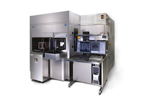
July 12, 2006 San Francisco, California, USA. Carl Zeiss SMT’s Nano Technology Systems division (Carl Zeiss NTS) and SII NanoTechnology Inc. (SIINT) jointly announce the launch of the XVision 300 Focused Ion Beam (FIB)/Scanning Electron Microscope (SEM) hybrid system during Semicon West 2006. XVision 300 is designed to enable demanding IC manufacturers for ultra-high resolution, 3-dimensional surface and sub-surface process inspection and defect analysis on 300mm wafers at the 65 / 45 nanometer design node and beyond. The workstation, which in particular enables for dissection of high quality TEM lamellas from anywhere of a 300mm wafer, represents the first jointly developed product emerging out of the strategic alliance between the two respective market leaders in electron and ion beam technology.
Based on an innovative high-performance automated 300mm Double Beam / Triple Beam platform, the XVision 300 combines the ultra-high resolution GEMINI® SEM imaging capabilities from Carl Zeiss NTS with ultra-high precision and high current FIB cutting capabilities from SIINT. Inheriting numerous automated and user-centric functionalities for nano-scale analysis, metrology and materials characterization, the XVision 300 represents an unprecedented versatile workstation. Thus XVision 300 enables both, cleanroom process monitoring as well as wafer-level defect root cause analysis in laboratory environments.
Main Product Features
Real-time SEM imaging capabilities during FIB milling
By utilizing the unique optical properties of Carl Zeiss NTS’ proprietary GEMINI® SEM technology, the XVision 300 allows for ultra-high precision control of the FIB cutting process during FIB operation in real time. This unique capability allows for highest precision FIB cuts of sub-surface sample features and defects, thereby substantially easing the overall tool operation and reducing time to result for high-throughput defect inspection, analysis and sample preparation for further analysis.
High quality TEM lamella preparation
An innovative new process feature offered by the XVision 300 is the application of a low-energy Gallium ion beam during final FIB polishing, thereby reducing any sample surface damage occurring during preparation of lamellas for transmission electron microscopy (TEM) to the demands of close-to atomic resolution TEM requirements. An additional low-energy Argon ion beam column (Triple Beam concept) can be installed on the XVision 300 series for additional removal of amorphous surface layers, thereby achieving unprecedented TEM lamella quality for quantitative atomic resolution TEM characterization. The newly designed SIINT FIB ion optics offers high beam current for almost doubling the throughput compared to conventional FIB systems. It offers a seamless support for full process control workflow ranging from high-rate abrasive Gallium FIB milling to Argon-based FIB fine polishing to final end-point detection by high resolution SEM imaging during ion milling and polishing.
Wide range of automated measurement functions
XVision 300 offers highly efficient process automation and data analysis capabilities at minimum operator interaction, comprising a wide variety of automated functions and programs such as its multiple-site TEM lamella preparation software (A-TEM). Further options include the even-distance cross-sectioning program, a highly accurate 3D image reconstruction capability for in-depth 3D feature analysis and fully automated cross-section image acquisition software (Auto Cut & See). Auto Cut & See allows the operator to create a process recipe in advance of the actual operation and enables for unattended acquisition of multiple sample sites in terms of automated FIB cross sectioning and auto-focus image recording. This feature strongly supports users in periodically and frequently revisiting critical wafer sites in a fully automated and controlled manner.
Powerful sample handling options
XVision 300 offers both FOUP as well as standard wafer holder handling options. The FOUP loader is designed to accommodate an additional TEM lamella extraction port which allows for unloading of TEM lamellas without unloading the wafer itself.
Dr. Hiroyuki Funamoto, President & CEO of SIINT, said:”Following the official announcement of our strategic alliance a few months ago, we are very proud to present the jointly developed XVision 300 today. This major achievement is the result of our joint innovation power and the hard work of people behind our products, clearly underlining the vibrancy of our collaboration.”
Dr. Dirk Stenkamp, Managing Director of Carl Zeiss SMT’s Nano Technology Systems division, states:”With its unique features, XVision 300 will enable our customers to rapidly adopt to the drastically increasing requirements of the 65 and 45 nanometer design node and beyond. Based on our joint core competencies in cutting-edge electron and ion beam technology, the XVision 300 represents our first building block of our joint new nano technology solutions portfolio, with other products to follow in the near term future.”
Contact Information
Press Contact
SII NanoTechnology Inc.
Corporate Communications Group
Tel: +81-3-6280-0061
Product Inquiry
SII Nanotechnology Inc.
FIB Sales / Marketing Mepartment
Tel: +81-3-6280-0065