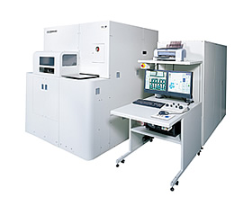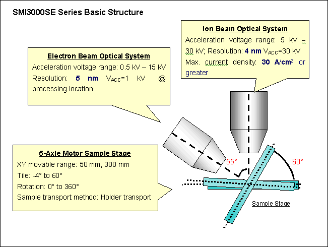
SII Nanotechnology Inc., a subsidiary of Seiko Instruments Inc. (SII), will release on December 1 two new models of the SMI3000SE series that combine FIB (Focused Ion Beam)*1 technology, with SEM (Scanning Electron Microscope) technology. These new models are compatible with large wafer samples: the SM13200SE for 200 mm wafer, and the SMI3300SE for 300 mm wafer. Delivery of SMI3300SE to major domestic semiconductor device manufacturers will begin in December, and will extend its distribution to the global market in 2005.
With semiconductor device, miniaturization and high integration to 65 or 45 nm nodes level are accelerated along with the increase in wafer size. Accordingly, semiconductor device manufacturing process management has reached the atomic level, and the TEM (Transmission Electron Microscope)*2 has become widely employed in such manufacturing process management, resulting in FIB use in sample preparation for TEM observation. At present, ultra-thin TEM samples of 50 nm or less are in demand, particularly when high-resolution observation is to be performed. To meet this demand, SMI3200SE and 3300SE permit minute cross-sectional processing and observation of selected area on a sample, and support fabrication of high-grade TEM samples.
Nanotechnology is expected to bring about innovations in many industries such as biotechnology. FIB technology capable of fabricating 3-D ultramicroscopic shapes on a nanometer scale is now recognized as essential to the research and development of nanotechnology, heightening expectations for its applications.
The SMI3000SE series is now comprised with three models: SMI3050SE released in spring this year, SMI3200SE and SMI3300SE, and compatible with wafer samples sized 50, 200, and 300mm.
[Main Features of SMI3200SE and SMI3300SE]
(1) Automatic Cut & See function
This feature is effective when performing automatic cross-sectional processing of selected area on a wafer with FIB and automatically conducting SEM cross-sectional observation. In addition to allow the user to review the automatically obtained cross-sectional images one by one, the feature enables three-dimensional observation when combined with 3D visualization software.
(2) Continuous A-TEM
This feature enables automatic TEM sample fabrication of multiple selected areas on a wafer when the processing recipe is registered in advance. The feature permits unattended continuous automatic processing at night, thereby improving throughput, enhancing operability and greatly reducing total cost.
(3) Real-time high-resolution FE-SEM observation
This feature enables real-time high-resolution SEM observation of the FIB processing status at all times. The feature is utilized with TEM sample fabrication as well as cross-sectional SEM observation and elemental analysis.
(4) Linkage with external systems
The positional coordinate linkage function which links the system with defect/failure inspection systems, CAD navigation systems and optical microscopes enables simple identification of processing locations.
(5) Micro-probing system
The micro-probing system allows the user to perform versatile probing operations of nanometer precision in a vacuum chamber.
[Price]
SMI3200SE unit: From 160 million yen
SMI3300SE unit: From 290 million yen
[Target sales amount]
First year for both models: 10 units
[Sale start date]
December 1, 2004
[Note]
*1: Focused Ion Beam (FIB) System
FIB System finely focus the ion beams of liquid metal gallium to a point of a few nanometers in size and, using the beam, scan sample surfaces, thereby enabling [1] sample observation, [2] cutting processes and [3] metal film formation processing on a nanometer scale. FIB Systems are mainly used in the field of semiconductor development and manufacture. SII NanoTechnology pioneered in development and sales of FIB System. It was the first company to deliver the FIB System for semiconductor device analysis in 1986, and the world’s first FIB-SEM hybrid system in 1990. SII NanoTechnology has delivered over 500 units of FIB System nationally and internationally, and currently holds the top share of the FIB System domestic market.
*2: Transmission Electron Microscope (TEM) and TEM Samples
The transmission electron microscope applies accelerated and focused electron beams onto a sample and amplifies the transmitted electrons using an electron lens, obtaining image information related to the internal structure of the substance. The flat surface resolution provided by the system offers observation at the highest among microscopes, enabling atomic level observation. However, since the system is based on a transmitted image, use of a thin sample with the TEM is a major prerequisite.
[About SII NanoTechnology]
SII NanoTechnology, a subsidiary of Seiko Instruments, Inc., is a world leader in the development of advanced, cutting edge measurement and analysis instruments. Its headquarters are located in Chiba prefecture, Japan. The company, the former Scientific Instruments Division of Seiko Instruments Inc., was established in December 2003. It was the first Japanese company to produce SPM and Focused Ion Beam (FIB) Systems. The company’s products line-up also includes XRF Analyze, XRF Coating Thickness Gauge, Thermal Analysis System, ICP-OES, ICP-MS and Mask Repair System. Many of these products are utilized to support leading edge research and development.
Additional information about the company is available on the internet at http://www.siint.com/en
SII NanoTtechnology Inc. Web website:http://www.siint.com/

Contact Information
Press Contact
Seiko Instruments Inc.
Corporate Communications Dept.
Io
Fax:+81-43-211-8011
Product Inquiry
SII Nanotechnology Inc.
FIB Sales / Marketing Department
Tel: +81-43-211-1345
Fax: +81-43-211-8067