Tokyo – April 11, 2006: SII NanoTechnology, Inc. (SIINT) announced today that it is releasing the “SmartMRC” mask rule checker. This product is a software package for mask data verifications, which is required for manufacturing and inspection of the photomasks used in leading-edge semiconductor devices. “SmartMRC” was jointly developed with Dai Nippon Printing Co., Ltd. and will be available from April 2006.
The aggressive OPC(*1) and advanced RET(*2) techniques are now used to deal with the lithographical limitations due to the ever finer feature sizes in recent semiconductor devices. As the number of fine patterns increases and the volume of data grow, the quality requirements on photomasks are becoming demanding. This causes to take longer times for mask manufacturing and inspection, which may increase costs and delivery times. “SmartMRC” is a software tool to detect potential problems in the mask manufacturing and inspection processes by extracting and checking the mask design data prior to the manufacture. This advanced data verification reduces mask manufacturing defects and falsely detected errors during mask inspection. As a result, “SmartMRC” contributes to reducing the mask cost and the delivery time.
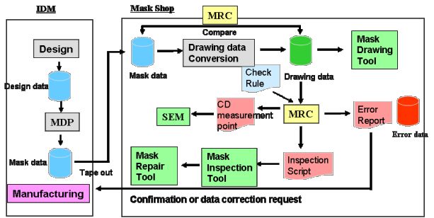
[Functions]
(1) Limit check function for mask drawing and inspection
(2) SEM(*3) measurement point extraction for verifying pattern uniformity in the manufactured mask
(3) Internal data checks during mask data conversion and mask data substitution
[Features]
(1) Direct input of the mask drawing data without GDS format(*4) conversion
(2) Reversed pattern checking without any data conversion
(3) Distributed computing available for linear speedup by parallel processing with a few tens of processors.
[Price]
Basic package: Starting from 30 million yen per CPU
Terminology
(*1): Aggressive OPC (Optical Proximity Correction)
A technology that repairs, in advance, for the deformations that occur when transferring the mask pattern to the wafer. As semiconductor rules become finer, the OPC patterns become more complex (aggressive).
(*2): RET (Resolution Enhancement Technique)
A technology that improves the resolution in semiconductor lithography.
(*3): SEM (Scanning Electron Microscope)
Scanning electron microscopes are used for measuring pattern dimensions.
(*4): GDS Format
A standard CAD data format used in the semiconductor industry.
Contact Information
SII NanoTechnology Inc.
Corporation Communications Group
Online Inquiry
http://www.siint.com/en/contact/index.html