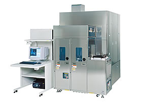
SII NanoTechnology Inc., a subsidiary of Seiko Instruments Inc. (SII), will release in April the photomask defect repair system “SIR7000FIB,” a system that repairs defects on photomasks for semiconductor devices which accommodate the 65-nm node. This system is a next generation system offering the ease-of-use of the photomask defect repair system “SIR5000” released in January 2003 for the 90-nm node, while realizing 65-nm node resolution and accuracy as well as reducing damage.
The “SIR7000FIB” model to be released was developed based on the technological accomplishments through joint research by Semiconductor Leading Edge Technologies, Inc., Dai Nippon Printing Co., Ltd., Toppan Printing Co., Ltd. and Hoya Corporation.
The photomask is an original plate used in the lithography process for making semiconductor circuits. In recent years, the photomask has emerged as a major factor in determining semiconductor element performance and production yield. In general, the following three technologies are critical to photomask production: (1) the technology used to form a pattern on a blank (a mask substrate covered with light shielding layers), (2) defect inspection technology used to detect whether the pattern formed as indicated by data, (3) and defect repair technology used to repair a defective pattern. The defect repairs performed include white defect repairs in which carbon is deposited in an area where a portion of the pattern is missing (white defect*1), and black defect repairs in which extraneous material that exists in a section where light is to be transmitted (black defect*1) is removed by etching. The photomask defect repair system repairs both black and white defects, thereby greatly improving the mask yield and making the system critical technology for mask production. With the 65-nm node generation, the size of defects requiring repair has become extremely small and complex in shape due to decreased line width and greater use of OPC patterns.*2 Also, due to the use of 193-nm ArF lithography,*3 the optical characteristics of the repair area have become extremely strict, requiring a reduction in glass damage to the degree of several nm.
SIR7000FIB is a system that repairs microscopic defects using focused ion beams (FIBs). The system is capable of repairing microscopic black and white defects of 60 nm or less, which is required with 65-nm node generation, to an accuracy of 10 nm or less (1 nm is 1-billionth of 1 meter), and repairing defects based on high transmission with reduced glass damage.
SII NanoTechnology sold the world’s first FIB-based photomask defect repair system in 1985, and maintains a high industry share both domestically and internationally. The new SIR7000FIB model is to be sold to photomask manufacturers both domestically and internationally.
[SIR7000FIB Main Features]
1. 10-nm or less (3σ) repair accuracy
The new system features improved repair accuracy, from the conventional 15 nm (3σ) to 10 nm (3σ). A new ion beam optical system improves ion beam radiation position stability and sharpens the beam focus, thereby enabling detailed observation of microscopic defect shapes. As a result, the system is capable of identifying and repairing defect shapes with higher fidelity. In addition, with a temperature control system mounted in the chamber unit to reduce temperature variance, the new system exhibits a reduction in temperature dependent drift.
2. CAD linkage function
By identifying the normal pattern of a defect area from the graphic data of EB*4 used in semiconductor layout design and superimposing the pattern on the defect area, the system enables repair based on a shape designed as close as possible to the normal pattern. The system also enables repair of complex shapes such as OPC shapes with higher fidelity.
3. SMIF transport mechanism
The new model utilizes a photomask SMIF transport mechanism. The system can load a photomask carried by an SMIF pod*5 into the chamber via a super clean load mechanism, preventing the adherence of particles (microscopic contaminants) to the photomask.
[Price]
SIR7000FIB unit: 550 million yen
[Sale Start Date]
April 15, 2005
[Notes]
*1 White defect, black defect
A “white defect” refers to a transparent area where the pattern is missing, and a “black defect” refers to an opaque area where the pattern was unnecessarily applied.
*2 OPC pattern
An “OPC pattern” refers to a pattern based on optical proximity correction. This technology involves preliminary correction to a pattern on the photomask side in order to ensure that the transferred pattern after exposure will be the pattern desired.
*3 ArF lithography
The name of a process in which the pattern on a photomask is exposed onto a wafer by reduced projection using the light source of an ArF (Argon Fluoride) excimer laser of a wavelength of 193 nm.
*4 EB
The abbreviation of “Electronic Beam.” Here, EB refers to electronic beam lithography equipment.
*5 SMIF pod
Mask storage container/box.. The SMIF pod is used to maintain a high degree of cleanliness inside the container/box and prevent the adherence of particles (microscopic contaminants).
[About SII NanoTechnology]
SII NanoTechnology, a subsidiary of Seiko Instruments, Inc., is a world leader in the development of advanced, cutting edge measurement and analysis instruments. Its headquarters are located in Chiba prefecture, Japan. It was the first Japanese company to produce SPM and Focused Ion Beam (FIB) Systems. The company’s products line-up also includes XRF Analyzer, XRF Coating Thickness Gauge, Thermal Analysis System, ICP-OES, ICP-MS and Mask Repair System. Many of these products are utilized to support leading edge research and development.
Additional information about the company is available on the internet at http://www.siint.com/en/
Contact Information
Press Contact
Seiko Instruments Inc.
Corporate Communications Dept.
Io
Fax:+81-43-211-8011
Product Inquiry
SII Nanotechnology Inc.
Mask Repair Sales Section
Watanabe, Matsumoto, Miyata
Tel: +81-43-211-1348